Materials Research
In his biography “Physics and Beyond” Werner Heisenberg reports from conversations in the early days of quantum mechanics. It was the general consensus that after working out the basic rules for understanding the atomic structure of matter, these “only” had to be applied to chemistry and biology in order to arrive at a similarly fundamental understanding as in physics. Well then, for almost 100 years the natural sciences have dedicated themselves to this program and have provided overwhelming and inspiring insights. But we are still not finished – there still is a lot of research to do to understand chemical and biological materials in order to get closer to the hope cherished by Heisenberg and colleagues.
Thin Films
are at the forefront of materials research and many high-tech applications. In most coating processes thin films are deposited atom by atom on a substrate. It is evident that the physics and functionality of the film will depend sensitively on the relative arrangement of atoms, that is their structure and morphology. The structure-forming processes of thin films can be devided into (1) surface-related processes and (2) bulk-related ones. Both processes cause pronounced preferred orientation of crystallites in polycrystalline films and lead to growth-related stress fields, the both of which may significantly influence the intended film functionality. The wavelengths of x-rays are of the same order of magnitude as typical interatomic distances, i.e. in the 0.1 nm range. Hence, x-rays are used as an effective probe to determine the local structure within thin films (chapter in ITC vol. H) and to study
- chemical phases and composition,
- preferred orientation (texture),
- grain sizes and microstrains,
- macrostrain associated with residual stress,
- thin film density and voids or void networks.
With these data the thin film technologist disposes of important information to elucidate the mechanisms that make the film grow and to tailor the film growth in order to achieve the intended properties.
Crytallography
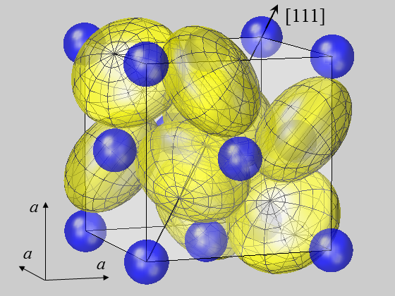
The calculation of crystal properties often makes use of a spherical modeling of atoms on their crystal lattice sites. But the question is: are atoms always as round as a sphere? Strictly speaking, the approach is only justified for atoms and ions on positions of high symmetry like in the fcc lattice or the NaCl structure. In most crystal structures, however, atoms reside on positions of lower symmetry, where a significant deviation of electron density from the shape of a sphere may arise.
This holds for many crystals that serve in high technology applications like piezo- or ferroelectrics, high-k dielectrics, photovoltaics and many others. For crystal constituents on polar positions (point group symmetry C1, Cs, Cn, Cnv, n = 2, 3, 4, 6) induced dipole moments may be elicited [13] that are of importance for the crystal energy [9, 15], the calculation of pyro- and piezoelectric constants [14] or the optical absorption coefficient [11]. It may generally be stated that atoms on these positions represent a key issue in understanding anisotropic crystal properties. It has recently been shown how the concept of ionic radii has to be extended and that anions should appropriately be modelled by ellipsoids rather than by spheres. For the case studies of pyrite-type compounds, ellipsoidal deformations were shown to occur for S ions in disulfides MS2 [48] and, more generally, for chalcogen ions X in dichalcogenides MX2 [62].